ECE 209 Midterm Notes
Materials Structures
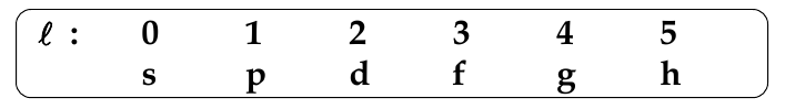
Crystalline, polycrystalline, and amorphous
-
materials can be classified into the 3 types: crystalline, polycrystalline, and amorphous
Crystalline
-
crystalline solid:
a solid in which atoms bond in a regular pattern to form a periodic array of atoms
-
long range order:
happens in a crystalline solid b/c periodicity;
-
means that each atom is in the same position relative to its relative
-
perfect order yay
Polycrystalline
-
long-range order exists over small distances only
-
has small crystal “grains” that are randomly oriented
Amorphous
-
no long-range order! It’s completely disordered
Crystals in microelectronics
-
different types of crystals should be used for different things in microelectronics
-
Polycrystalline silicon used for:
-
gate material in MOS transistors
-
interconnect lines
-
Amorphous silicon used for:
-
switching transistors for AMLCD displays
-
solar cells
-
crystalline used for all kinds of things
-
attractive because of perfect order, which:
-
simplifies theories
-
repeatable, predictable and uniform properties for material processing
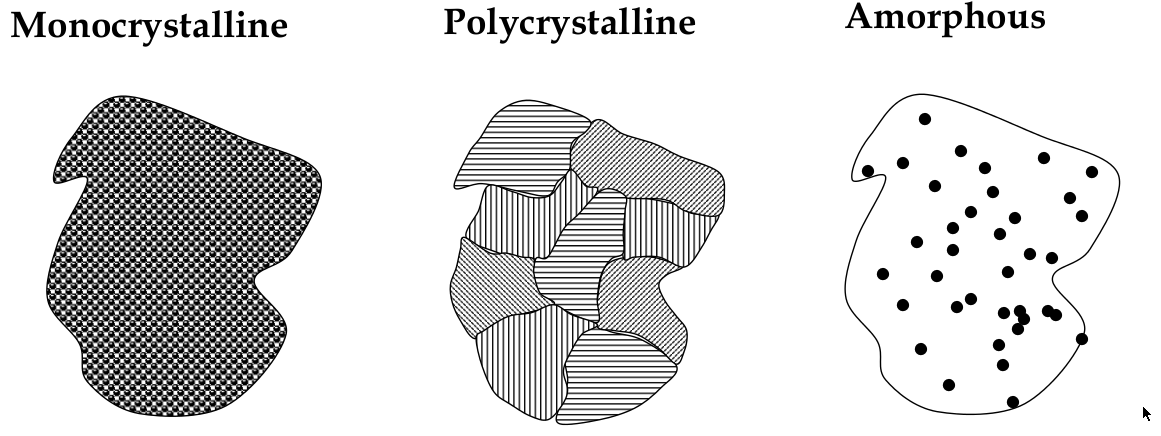
Silicon structure; covalent bonding
-
covalent bonding: shares atoms to make a full valence shell (8 atoms for Si)
-
Si ends up in a tetrahedral shape due to the repulsion interactions
-
silicon has a diamond unit cell
Unit cell
-
lattice:
infinitely repeating array of geometric points in space
-
lattice crystal structure:
a lattice, with atoms on the lattice points
-
unit cell:
smallest repeating structure in the lattice crystal structure
-
lattice constant:
the length of the cubic unit cell - a
-
interatomic distance:
the distance between atoms in a unit cell (not the same as a!!)
Bragg’s Law
-
to measure the lattice constant of an atom, use x-ray diffraction
-
for a wave incident on a plane of atoms, reflective pattern will have bright and dark spots from constructive and destructive interference
-
Bragg’s Law for where bright spots appear:
$$ n\lambda = 2dsin\theta $$
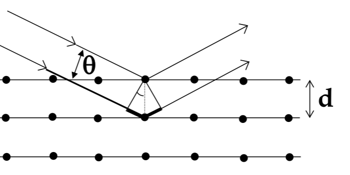
- crystal characteristics (and x-ray diffraction) depend on the direction you are looking
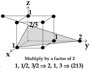
Miller indices
-
since direction matters, we need a way of classifying it
-
miller indices: sets of 3 numbers that are used to identify groups of crystal planes and directions
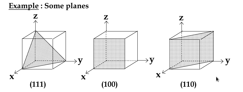
Miller Indices for Planes
-
set up 3 axes along 3 adjacent edges of unit cell
-
choose unit cell length as unit distance along respective axis (a = 1)
-
chose a plane that passes through the centre of particular atoms. The plan intersects the axes at distances x1,y1, za (in example below, 1,2, 2/3)
-
take reciprocals of interception co-ordinates, change to set of smallest ints, write as (hkl)
Miller Indices for Directions
-
take a parallel line which passes through the origin
-
not the length of the projections of this line on x,y,z axes
-
change to smallest ints
-
write as [hkl]
Family of Planes and Directions
-
family of planes: {hkl)
-
family of directions:
-
represents all equivalent planes/directions
-
{110} represents all planes (110), (011), (101), etc
Transmission Electron Microscopy
-
TEM samples thinned and illuminated with accelerated electrons
-
electrons are absorbed in the sample depending on thickness and material composition
-
intensity variation of the transmitted electron beam is observed using a viewing screen
Scanning Tunneling Microscopy
-
scans across the surface of sample with a very sharp needle
-
needle kept 1nm from surface, voltage applied between needle and sample
-
current used as feedback signal to determine gap size (can only give information about surface of sample)
Silicon bulk crystal growth
-
to make ICs, we have to grow perfect crystals on a commercial scale
-
for crystal growth, a saturated solution or a molten liquid is usually used.
-
the material is then grown on a
seed
crystal which acts as a
template
for the new growth
-
for silicon:
-
raw material: silicon dioxide
-
reduction => metallurgical grade polycrystalline Si
-
purification => electronic grade polycrystalline Si
-
melting & growth => crystalline bulk Si
-
during melting and growth, a seed crystal is pulled slowly out of a bath of molten and rotated slowly
-
this is Czochralski (Cz) crystal pulling
-
after growth, ingot is trimmed and sliced into wafers

Epitaxial growth
-
electrical properties of Si are controlled roughly when the basic wafers are produced, but more precise cotrol is needed for reliable devices
-
the top few microns of the wafer are where devices are made
-
this region must be well controlled
-
achieved by growing a even more perfect crystal layer on top of the wafer
-
called the
epitaxial layer
-
during epitaxial growth, the surface of the wafer acts as the template
-
decomposes Si-containing gases in chemical vapor dposition
-
monolayer
: a layer one atom thick
Molecular beam epitaxy
-
a technique for growing thin layers
-
a steam of neutral atoms or molecules are evaporated from a heated cell
-
then incorporated into the growing film onto a heated target
-
is
$$$
$ b/c:
-
only one wafer can be used at a time
-
wafer must be small to get uniform layer
-
very good vacuum required
Epitaxy principles
-
major feature of epitaxy is that the newly deposited film precisely follows the crystalline form of the substrate template
-
adsorption: proces of atoms attaching themselves to the surface
-
adsorption can occur anywhere on the surface with equal probability, so layer is unlikely to be crystalline
-
for crystalline growth, absorbed atoms must be able to find the
minimum energy positions
-
the ad-atoms must be able to move along the surface
-
heat up the substrate during epitaxy to allow movement
-
if not hot enough, the ad-atoms stick where they land and the film is amorphous
Modifying Crystals
-
to make an electronic device, crystals need to be modified and shaped according to the needs of the device
-
examples: introducing impurities, etching/shaping
Ion implantation
-
ionized impurities are accelerated into an electric field and “smashed into” Si surface
-
depth of penetration determined by:
-
accelerating voltage
-
masses of ions and target atoms
-
crystal direction (density of atoms)
Etching and micromachining
-
sometimes you need to etch crystals to get certain structures
e.g. for making DRAMs, you need to etch deep tranches to make trench-capacitors
-
wet-etching: uses liquid chemicals to remove materials from a wafer
-
isotropic etching: chemicals etch at the same rate in all directions
-
anisotropic etching: chemicals selectively etch one crystal plane more
-
see example below. KOH etches (100) faster than (111) planes

Atomic Structure
Nature of light
-
classic physics: light is an electromagnetic wave w/ perpendicular field Bx and Ey
-
electric field is given by the following equation:
$$ E_y = E_o sin(kx - \omega t) $$
-
where:
-
k = 2π/λ - the wavenumber (λ is the wavelength of light)
-
ω = 2πf - the angular frequency (f is the freq of light)
-
c= ω/k = fλ - speed of light / wave velocity
-
light intensity is given by:
$$ I = \frac{1}{2} c \epsilon_o E_o^2 $$
Experimental Evidence of Light as EM Wave
-
interference and diffraction
-
Young’s double-slit experiment
Photo-emission (photoelectric effect)
-
when a metal electrode is illuminated with light, it emits electron (can create a current with this!)
-
light must possess the energy needed to “free” the electron from the metal (W)
-
any excess energy it possesses will become the kinetic energy of the electron
-
according to classical theory of light, the energy balance should be: E
L
= W + E
K
-
if we reduce E
L
by reducing the intensity of the light, E
K
should also decrease
-
if light intensity is increased -> saturation current increases
-
more electrons emiited
-
same voltage is required to stop the current, thus the kinetic energy of the electrons is the same
-
classical theory of light can’t explain this!
Photons
-
light contains particle of fixed energy called
photons
-
light frequency increases -> energy of light increases
-
E
L
= hf
Wave-Particle Duality
-
light has properties of both a wave and a particle
-
light waves consist of a stream of photon particles, each with energy hf
-
energy carried by the wave consists of
discrete lumps
or
quanta
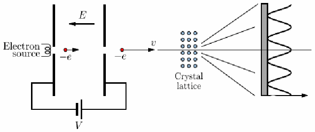
De Broglie relationship
-
electrons also have a wave-particle duality
-
particle-like properties confirm with cathode ray tube (1897)
-
deBroglie predicted that electrons would have a wavelength:
$$ \lambda = \frac{h}{p} $$
-
where p = mv is the electron momentum
-
confirmed with electron diffraction experiment
Electron Diffraction Experiment
-
voltage accelerates electron, strikes a thin carbon layer, hits the screen
-
produce a glow of light proportional to their number and energy
-
using this, get the deBroglie relationship
Wavefunction, wave vector, and Schrödinger equation
-
for an electromagnetic wave:
$$ E_y (x,t) = E_o sin(kx - \omega t) $$
-
for an electron wave:
$$ \psi = A sin(kx - \omega t) $$
$$ \psi = Ae^{j(kx - \omega t)} $$
-
where:
-
k = 2π/λ - the wave vector
-
ω = 2πf
-
A = constant
-
can separate the time-dependent and space-dependent parts and write:
$$ \psi = Ae^{jkx}e^{-j\omega t}$$
-
wave function related to the
probability
of finding the electron at a given point in space and time
-
represents the distribution of the electron wave in time
-
Probability = ΨΨ* = |Ψ|
2
-
probability is a real value
Wave Vector and Potential Energy
-
electron wave momentum is related to the wavelength by this equation: p = h/v
-
momentum is a vector - therefore we need a vector form of the wavelength
-
wave vector:
-
direction: direction of wave travel
-
magnitude: k = 2π\λ
-
momentum now written as:
$$ p = \frac{h}{2π}k$$
-
kinetic energy is:
$$ E_k = \frac{p^2}{2m} = \frac{h^2}{8π^2}\frac{k^2}{m}$$
-
electron also has electrostatic potential energy
-
defined as the work done in pulling the negatively chargely electron from an infinite distance to a distance, r, from the positively charged nucleus:
$$ E_p = \frac{-e^2}{4πε_0 r} $$
-total energy is E = E
k
+ E
p
$$ k = \frac{2π}{h} \sqrt{2m(E - E_p)} $$
Schrodinger’s Equation
-
describes the electron wave function
-
if you know the electron potential energy and boundary conditions, you can calculate the parameters of electron orbital (wave function and energy)
$$ \frac{d^2 \Psi}{dx^2} + \frac{8\pi^2 m}{h^2}(E - E_p )\Psi = 0 $$
“Electron in a box” problem
Electron in a 1D Potential Well
-setup:
- inside the box, potential energy is zero
- outside, is infinitely large
- we need to find the wave equation
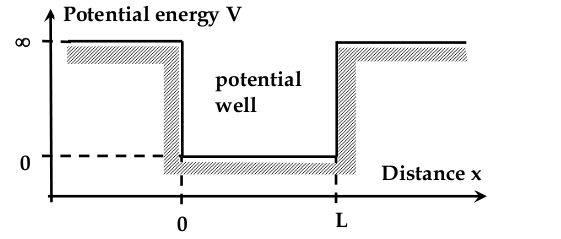
$$ \frac{d^2 \Psi}{dx^2} + \frac{8\pi^2 m}{h^2}(E - V)\Psi = 0 $$
-
assumptions:
-
the case is time-independent
-
wave function is continuous, smooth, and single-
-
Boundary conditions:
-
For x<0 and x>L, the term Vψ dominates
$$ -V\Psi = 0 \\
\Psi = 0
|\Psi|^2 = 0
$$
electron cannot be outside the well
-
Since d
2
ψ/dx
2
must be continuous, ψ = 0 at x={0,L}
-
Differential equation:
-
second order differential equation to solve for within the well
-
general solution equation is:
$$ \Psi (x) = 2Ajsin(\frac{n\pi x}{L}) $$
-
can solve for A because we know the probability of electron being in the box is 1 (integral of equation from 0 to L is 1)
-
final form of the equation is:
$$ \Psi (x) = j(\frac{2}{L})^{\frac{1}{2}}sin(\frac{n\pi x}{L}) $$
Electron Energy in Potential Well
$$ E = \frac{h^2 n^2}{8mL^2} $$
- energies E(n) are the eigenenergies of the electron
- energy is quantized
- n is the
quantum number
- min energy is at n=1, this is the
ground state
- energy of electron wave can only have discrete values
- energy of electron particle can take any value
Uncertainty Principle
-
free electron:
-
has single energy, momentum, wavelength - Δp = 0 (uncertainty 0)
-
electron wave is spread all over the space, so Δx = ∞
-
electron in a potential well:
-
Δx = L
-
Δp = hk/π
-
for n=1, k: = π, Δp = h/L
$$ \Delta x \Delta p = L \frac{h}{L} = h $$
-
Heinsenberg’s uncertainty principle: we cannot simultaneously and exactly know both the position and momentum of an electron along a given co-ordinate
Tunnelling
-
important application of the uncertainty principle
-
if an electron of energy E meets a potential energy barrier of height V_o_ > E, it might leak (“tunnel”) throug the barrier
-
probability of that depends on the energy and width of the barrier
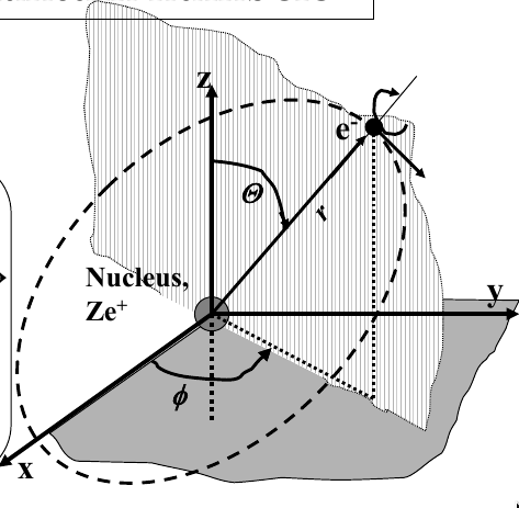
Hydrogen atom
-
consider the H atom: an electron attached to a nucleus
-
electron is electrostatically bound to a single proton
-
since proton is so big, it behaves more like a particle
-
potential energy:
$$ V(r) = \frac{-Ze^2}{4\pi \epsilon_o r} $$
-
where:
-
Z = number of electrons
-
r = (x
2
+ y
2
2 + z
2
)
1/2
-
considerng electron in H atom as confined in a potential well with PE V(r), electron’s wave function can be derived to be:
$$ E = \frac{-Z^2 e^4 m}{8h^2 \epsilon_o^2}\frac{1}{n^2} $$
-
different energy values (different values on) are called
Energy Levels
Atomic Spectra
-
electrons can be excited into higher energy levels - requires energy
-
they can also return to a lower levels - releases energy in the form of a photon with appropriate energy E = hf = E
higher
- E
lower
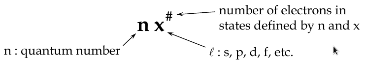
Quantum Numbers
Principal Quantum Number, n
-
determines the radius of electron orbit and the energy level
Orbital Angular Quantum Number, l
-
determines the shape of the orbital
-
the electron wave at each orbit (at each r) may be standing or moving along the orbit
-
wave must be continuous and smoothly varying
-
must fit an integral number of wavelengths: lλ = 2πr
$$ L = pr = \ell \frac{h}{2\pi} $$
-
L is the angular momentum, which is quantized.
-
l can take any value from 0 to (n-1)
Magnetic Quantum Number, m
l
-
determines orientation of the orbital in space (the tilt of the electron cloud), and the energy of its electron in a magnetic field
-
angular momentum about the electron orbit is quantized as:
$$ L_z = \frac{m_\ell h}{2\pi} $$
-
-l ≤ m
l
≤ l
Electron Spin Quantum Number, m
s
-
determines the rotation of electron about its own axis
-
has the values 1/2, -1/2 (spin up, spin down)
The Full Sert of Quantum Numbers and Values
n = 1, 2, 3, … z
l = 0, 1, 2, 3, … (z-1)
m
l
= 0, ±1, ±2, ±3, … ±(z-1)
m
s
= ±1/2
Summary of Quantum Numbers
-
Radius of orbit → n
-
Orbital angular momentum → l
-
Tilt of orbit’s plane → m
l
-
Spin of electron → m
s
Electron Clouds
-
we can define electron clouds corresponding to different combos of quantum numbers
-
probability density distribution
Multi-electron atoms, Pauli principle, and the periodic table
Band Structure
Hydrogen molecule and molecular bonding
-
when atoms interact, they change behaviour
-
no two electrons in an interacting systems may occupy same quantum state
-
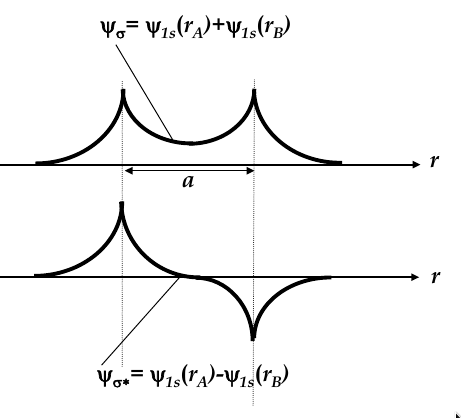
consider the case of two H atoms
-
when they are infinitely far apart, they have the same wave function
-
when they approach each other, their wave functions overlap and two new
molecular wave functions
emerge (see the image below for the two new functions
-
molecular wave functions are linear combinations of atomic orbitals; in this case, one is the sum and one is the difference
-
Ψ
σ
is more confined to the nuclei, whereas Ψ
σ*
is more spread
-
thus, Ψ
σ*
has higher energy
-
Ψ
σ
then is more energetically favourable, so both electrons occupy this state
-
bonding orbital:
the wave function Ψ
σ
corresponding to the lowest energy level
-
antibonding orbital:
Ψ
σ*
-
total energy of two electrons in H
2
molecule is lower than in two single H atoms
-
one electron has to flip its electron spin but the energy gain due to dropping to bonding orbital is higher than the energy spent
-
consider 3 hydrogen atoms. They will also add their atomic wave functions, like so:
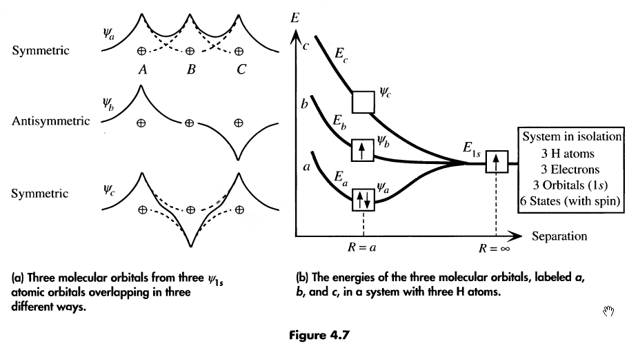
-
the more atoms in our function, the more molecular orbitals they’ll form. n atoms = n orbitals
-
if an energy band is not entirely filled, there are states available for electrons. Consider N Li atoms (2s half filled)
-
thermal energy is enough at room temp for electrons to jump between nearest energy levels
-
since the levels may belong to different atoms, electrons can easily travel from atom to atom
conducting current
Hybridization
-
2s and 2p energy levels are close, so when they approach each other, 2 2s and 2 2p orbitals can mix to form hybrid orbitals
-
hybrid orbitals directed in tetrahedral directions and have the same energy
-
process called
sp
3
hybridization
Energy Bands
-
when interatomic distance decreases so that electrons interact, their energy levels broadens (splits) into bands
-
there are 2N states in the 2s-band, 6N states in 2p-band
-
in diamond crystal, bonding and anti-bonding orbitals split and form
valence band
and
conduction band
, respectively
-
band gap - E
G
- the difference in energy between the conduction and valence bands
Fermi Energy
-
at T=0K, all electrons will occupy states with lowest energy (valence band), so conduction band empty
-
fermi energy (E
F
) = energy level corresponding to highest filled electron state at 0K.
-
as T increases, bands above E
F
start to get filled
-
to conduct electric current, there must be vacant states in the band
-
no states available in energy levels within each band, no conduction
need more but confusing tho
Effective mass
-
acceleration of an free electron in vacuum is a = F
ext
/ m
e
, m
e
= electron mass in vacuum
-
in a solid, electron interacts with crystal lattice atoms and experiences internal forces F
int
-
thus, acceleration is: a = (F
ext
+ F
int
) / m
e
-
since atoms in a crystalline solid are periodically positioned, variation of F
int
is also periodic, we can simplify our acceleration equation:
$$ a_crystal = \frac{F_ext}{m_e^*}
-
where m
e
2
is the
effective mass
of the electron
-
effective mass depends on the material
Electrons and holes
-
in semi-conductors, in order to get excited to empty states, electrons jump across the band gap
-
when excited to the conduction band, a vacant state is left in the valence band
-
this is called a
hole
- the absence of an electron
-
electrical conduction in a semiconductor involves movement of electrons in the conduction band and holes in valence band
-
electron and hole currents
Intrinsic Semiconductor
-
a pure semiconductor (no foreign atoms present) is an intrinsic semiconductor
-
electrons and holes can only be created in pairs (electron-hole pairs)
Carrier Generation
-
electron-hole pair generation: the act of exciting an electron from the valence band to the conduction band
-
electrons can be excited even though E
T
is much smaller than E
G
because atoms in the crystal are constantly vibrating (due to thermal energy) and
deforming interatomic bonds
-
thus, some bonds may be overstretched, and the bond energy can be smaller than thermal energy
-
electron concentration in the conduction band, n, (electrons per cm
3
) is always equal to hole concentration in the valence band, p, (holes per cm
3
)
-
n = p = n
i
-
n
i
= intrinsic carrier concentration
-
g
i
: rate of generation
Recombination
-
opposite of carrier generation: the act of an electron falling back to VB
-
excess energy is released in the form of heat or light
-
rate of recombination, r
i
, is proportional to equilibrium concentration of electrons/holes
-
r
i
= αn
0
p
0
= αn
i
2
-
α = constant
-
n
0
= equilibrium electron concentration
-
p
0
= equilibrium hole concentration
-
in steady state, r
i
= g
i
Conduction
-
takes place only when electron-hole pairs are created
-
conduction not great in intrinsic semiconductors at room temperature
Doping, extrinsic semiconductors
-
doping:
creation of carriers in semiconductors by introducing impurities
-
we get extra carriers, and better conductivity
-
doped semiconductor = extrinsic semiconductor
-
n-type semiconductor:
predominant electron concentration
-
p-type semiconductor:
predominant hole concentration
n-type doping
-
n-type Si obtained by adding small amounts of group V elements (P, As, Sb)
-
these elements have 5 valence electrons, but the atoms bond to Si (4 e
-
), so one of the electrons is
weakly
bonded to the impurity atom
-
very tiny amount of energy needed to excite electrons, so at most temperatures most of the donor electrons will be ionized
p-type doping
-
p-type Si obtained by adding small amount of group III elements (B, Al, Ga, In)
-
these elements have 3 valence electrons, atoms bond to Si (4 e
-
), one of the bonds will miss an electron
-
impurity atoms = acceptors (accept an extra electron)
Carrier concentration
-
how to calculate the number of electrons and holes available for conduction? need to know:
-
number of states available at a particular energy to be occupied
-
fraction of these states that are in fact occupied at a particular temperature
$$ n_o = \int_{E_c}^\infty \! f(E)N(E) \, \mathrm{d}E. $$
-
where:
-
N(E) - density of states
-
f(E) - Fermi function
Density of States
-
DOS: number of available states per unit volume
-
expressions for valence and conduction band are:
$$ N_V(E) = \frac{8\sqrt{2}\pi}{h^3}(m_p^*)^{\frac{3}{2}}(E_V - E)^{\frac{1}{2}} for E < E_V \\
N_V(E) = \frac{8\sqrt{2}\pi}{h^3}(m_n^*)^{\frac{3}{2}}(E - E_C)^{\frac{1}{2}} for E > E_C
$$
Fermi function
$$ f(E) = \frac{1}{1 + e^{\frac{E - E_F}{kT}}} $$
- Fermi-Dirac distribution function gives us the probability that an available energy state at E will be occupied by an electron at temperature T
-
probability that an available energy state will be occupied by a hole is 1 - f(E)
- at E=E
F
, f(E) = 1/2
- E
F
in intrinsic material: middle of band gap b/c concentration of holes in VB = concentration of electrons in CB
- E
F
in n-type material: closer to E
C
because the concentration of electrons in CB is higher than concentration of holes in VB
- E
F
in p-type material: close to E
V
because concentration of holes in VB is higher than concentration of electrons in CB
Equilibrium Carrier Concentration
-
for equilibrium conditions, can use the
effective density of states
* N
C
at energy E_C. Thus:
$$ n_0 = N_C f(E_C) $$
-
Then, f(E
C
) can be expressed as:
$$ f(E_C) = \frac{1}{1 + e^{\frac{E_C - E_F}{kT}}} = e^{-\frac{E_C - E_F}{kT}} $$
$$n_0 = N_C e^{-\frac{E_C - E_F}{kT}} $$
-
similarly, concentration of holes is:
$$ p_0 = N_V [ 1 - f(E_V) ] $$
-
where N
V
is the effective density of states in the valence band
-
$$ p_0 = N_V e^{-\frac{E_F - E_V}{kT}} $$
Mass Action Law
$$ n_0 p_0 = n_i^2 \\
n_0 = n_i e^{\frac{E_F - E_i}{kT}} \\
p_0 = n_i e^{\frac{E_i - E_F}{kT}} $$
Conductivity and mobility
-
current of electrons and holes depends on:
-
carrier concentration (n, p)
-
carrier speed (v
n
, v
p
)
-
carrier charge (q or e)
-
current density can be written as:
$$ J_n = nev_n \\
J_p = pqv_p $$
-
at low electric field, the carrier velocity is proportional to the field: υ = με
-
the proportionality constant μ is called the
mobility
-
total current density is: J = σε
-
ε is called the
conductivity
Hall Effect
-
mobility in semiconductors can be estimated using the Hall effect
-
if we apply electric field E
x
in direction x across a semiconductor and submit it to magnetic field B
z
in direction z, then another electric field E
y
(Hall field) occurs perpendicular to both E
x
and B
z
-
E
y
occurs due to deflection of electrons from direction z due to
Lorentz force
F
y
= -ev
x
B
-
electron velocity in x-direction: v
x
= μ
x
E
x
-
in steady state, deflection is steady and Hall field counterbalances Lorentz force:
-
eE
H
= ev
x
B
z
-
eE
H
= J
x
B
z
/n
-
E
H
/J
x
B
z
= 1/en = R
H
- Hall coefficient
-
μ = | σR
H
| - Hall mobility
Haynes-Shockley Experiment
-
direct way of measuring mobility
Temperature dependence of carrier concentration
$$ n_i (T) = 2{\frac{2\pi kT}{h^2}}^{\frac{3}{2}}{m_n^* m_p^*}^{\frac{3}{4}}e^{\frac{-E_G}{2kT}} $$
Compensation doping
-
semiconductor could have both acceptors and donors in it: this is compensation doping
-
the concentrations of electrons, holes, donors and acceptors can be obtained from
space charge neutrality law
-
the material must remain electrical neutral overall
-
p
0
+ N
d
+
= n
0
+ N
a
-
-
a material doped equally with donors and acceptors becomes “intrinsic” again
Diffusion Current
-
diffusion: net motion of carriers from regions of high carrier concentration to low carrier concentration if there is non-uniformity (gradient) of carrier concentration
need more
Direction and indirect bandgap semiconductors
-
dielectrics and semi-conductors behave essentially the same way - the only difference is the
bandgap width
-
photons with energy exceeding E
g
are absorbed by giving their energy to electron-hole pairs
-
may or may not reemit the light during recombination depending on whether the gap is
direct
or
indirect
-
direct bandgap
semiconductors: electron drops from bottom of CB to top of VB, excess energy emitted as a photon
-
also known as
radiative recombination
-
indirect bandgap
semiconductors: recombination occurs in two stages via recombination centres (usually defects) in the bandgap:
-
electron falls from bottom of CB to the defect level, then down to the top of VB
-
electron energy is therefore lost in two portions by the emission of
phonons
(lattice vibrations)
-
this process is also known as
non-radiative recombination
Photoconductivity
-
increase of conductivity under illumination
$$ \Delta \sigma = \sigma_photo - \sigma_dark = \frac{e\eta I\lamda \tau (\mu_e + \mu_h)}{hcD}
-
η is quantum efficiency, and τ is average excess carrier lifetime
Energy-band diagrams and MOSFET